- 您现在的位置:买卖IC网 > Sheet目录483 > NDD04N50Z-1G (ON Semiconductor)MOSFET N-CH 500V 3A IPAK
NDD04N50Z
N-Channel Power MOSFET
500 V, 2.7 W
Features
? Low ON Resistance
? Low Gate Charge
? ESD Diode ? Protected Gate
? 100% Avalanche Tested
? These Devices are Pb ? Free, Halogen Free/BFR Free and are RoHS
Compliant
ABSOLUTE MAXIMUM RATINGS (T C = 25 ° C unless otherwise noted)
V DSS
500 V
http://onsemi.com
R DS(on) (MAX) @ 1.5 A
2.7 W
Rating
Drain ? to ? Source Voltage
Continuous Drain Current R q JC
Continuous Drain Current
R q JC , T A = 100 ° C
Pulsed Drain Current, V GS @ 10 V
Power Dissipation R q JC
Gate ? to ? Source Voltage
Single Pulse Avalanche Energy,
I D = 3.4 A
ESD (HBM) (JESD22 ? A114)
Peak Diode Recovery
Symbol
V DSS
I D
I D
I DM
P D
V GS
E AS
V esd
dv/dt
Value
500
3.0
1.9
12
61
± 30
120
2800
4.5 (Note 1)
Unit
V
A
A
A
W
V
mJ
V
V/ns
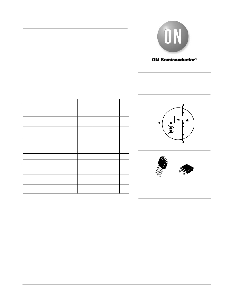
G (1)
N ? Channel
D (2)
4
S (3)
4
Continuous Source Current
(Body Diode)
Maximum Temperature for Soldering
Leads
I S
T L
3.4
260
A
° C
1
2
3
1 2
3
Operating Junction and T J , T stg ? 55 to 150 ° C
Storage Temperature Range
Stresses exceeding Maximum Ratings may damage the device. Maximum
Ratings are stress ratings only. Functional operation above the Recommended
Operating Conditions is not implied. Extended exposure to stresses above the
Recommended Operating Conditions may affect device reliability.
1. I D v 3.4 A, di/dt ≤ 200 A/ m s, V DD ≤ BV DSS , T J ≤ 150 ° C.
IPAK DPAK
CASE 369D CASE 369AA
STYLE 2 STYLE 2
MARKING AND ORDERING INFORMATION
See detailed ordering and shipping information in the package
dimensions section on page 6 of this data sheet.
? Semiconductor Components Industries, LLC, 2011
September, 2011 ? Rev. 1
1
Publication Order Number:
NDD04N50Z/D
发布紧急采购,3分钟左右您将得到回复。
相关PDF资料
NDD05N50ZT4G
MOSFET N-CH 500V 5A DPAK
NDF02N60ZH
MOSFET N CH 600V 2.4A TO220FP
NDF03N60ZH
MOSFET N CH 600V 4.8A TO220FP
NDF04N60ZH
MOSFET N CH 600V 4.8A TO220FP
NDF04N62ZG
MOSFET N-CH 620V 2OHM TO220FP
NDF05N50ZH
MOSFET N-CH 500V 4.4A TO-220FP
NDF06N60ZG
MOSFET N-CH 600V 7.1A TO-220FP
NDF06N60ZH
MOSFET N CH 600V 7.1A TO220FP
相关代理商/技术参数
NDD04N50ZT4G
功能描述:MOSFET 500V 3A HV MOSFET DPAK RoHS:否 制造商:STMicroelectronics 晶体管极性:N-Channel 汲极/源极击穿电压:650 V 闸/源击穿电压:25 V 漏极连续电流:130 A 电阻汲极/源极 RDS(导通):0.014 Ohms 配置:Single 最大工作温度: 安装风格:Through Hole 封装 / 箱体:Max247 封装:Tube
NDD04N60Z
制造商:ONSEMI 制造商全称:ON Semiconductor 功能描述:N-Channel Power MOSFET 1.8 , 600 Volts
NDD04N60Z-1G
功能描述:MOSFET NFET IPAK 600V 4A 1.8R RoHS:否 制造商:STMicroelectronics 晶体管极性:N-Channel 汲极/源极击穿电压:650 V 闸/源击穿电压:25 V 漏极连续电流:130 A 电阻汲极/源极 RDS(导通):0.014 Ohms 配置:Single 最大工作温度: 安装风格:Through Hole 封装 / 箱体:Max247 封装:Tube
NDD04N60ZG
制造商:ON Semiconductor 功能描述:NDD Series 600 V 1.8 Ohm 83 W Surface Mount N-Channel Power MOSFET - TO-252-3
NDD04N60ZT4G
功能描述:MOSFET NFET DPAK 600V 4A 1.8R RoHS:否 制造商:STMicroelectronics 晶体管极性:N-Channel 汲极/源极击穿电压:650 V 闸/源击穿电压:25 V 漏极连续电流:130 A 电阻汲极/源极 RDS(导通):0.014 Ohms 配置:Single 最大工作温度: 安装风格:Through Hole 封装 / 箱体:Max247 封装:Tube
NDD04N62Z
制造商:ONSEMI 制造商全称:ON Semiconductor 功能描述:N-Channel Power MOSFET 620 V, 1.8
NDD04N62Z-1G
制造商:ONSEMI 制造商全称:ON Semiconductor 功能描述:N-Channel Power MOSFET 620 V, 1.8
NDD04N62ZT4G
制造商:ONSEMI 制造商全称:ON Semiconductor 功能描述:N-Channel Power MOSFET 620 V, 1.8
